
Downloaded from hlayiso.com
NATIONAL
SENIOR CERTIFICATE
GRADE 12
SEPTEMBER 2022
ELECTRICAL TECHNOLOGY: ELECTRONICS
MARKS: 200
TIME: 3 hours
This question paper consists of 18 pages, including a 2-page formula sheet.
Skip to contentAll 2022 papers 
View all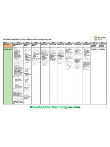
Electrical Technology Grade 12 Eastern Cape Mock 2022 QP
Grade 12 Electrical Technology question paper from the Eastern Cape Mock Exam 2022 (English), 18 pages. Read online or download the free PDF.
Electrical Technology · Grade 12 · Eastern Cape Mock Exam · 2022 · English. Question paper, 18 pages. Read online or download the PDF.
- Subject
- Electrical Technology
- Grade
- Grade 12
- Language
- English
- Document type
- Question paper
- Year
- 2022
- Exam period
- Eastern Cape Mock Exam
- Curriculum
- CAPS
- Pages
- 18
- File size
- 428.0 KB
Free to read online, no sign-up needed
Loading document…
Loading document…
1 of 18
This exam
Document textSearch extracted text and jump to a page.
Downloaded from hlayiso.com
2 ELECTRICAL TECHNOLOGY: ELECTRONICS (EC/SEPTEMBER 2022)
INSTRUCTIONS AND INFORMATION
1. This question paper consists of SIX questions.
2. Sketches and diagrams must be large, neat and FULLY LABELLED.
3. Show ALL calculations and round off answers to TWO decimal places.
4. Number the answers correctly according to the numbering system used in
this question paper.
5. You may use a non-programmable calculator.
6. Show the units for ALL answers of calculations.
7. A formula sheet is provided at the end of this question paper.
8. Write neatly and legibly.
Copyright reserved Please turn over
Downloaded from hlayiso.com
(EC/SEPTEMBER 2022) ELECTRICAL TECHNOLOGY: ELECTRONICS 3
QUESTION 1: MULTIPLE-CHOICE QUESTIONS
Various options are given as possible answers to the following questions. Choose
the answer and write only the letter (A–D) next to the question numbers
(1.1 to 1.15) in the ANSWER BOOK, for example 1.16 D.
1.1 The purpose of the Occupational Health and Safety Act is to …
A provide for the health and safety of persons at work.
B provide for the health and safety of persons at home.
C prevent wear and tear on machinery.
D prevent workers from using machinery. (1)
1.2 In a parallel RLC circuit …
A 𝐼𝐿 = 𝐼𝐶 = 𝐼𝑅 .
B 𝑋𝐿 = 𝑋𝐶 = 𝑅.
C 𝑉𝐿 = 𝑉𝐶 = 𝑉𝑅.
D 𝑉𝑇 = 𝐼𝑇 = 𝑍𝑇. (1)
1.3 The capacitance of a capacitor with a capacitive reactance of 31,83 Ω when
connected to a 110 V/50 Hz supply is:
A 10 ɥF
B 100 ɥF
C 100 nF
D 10 nF (1)
1.4 The bandwidth of a series resonant circuit is … affected by its quality factor.
A not
B indirectly
C directly
D negatively (1)
1.5 The FET relies on the creation of an …
A electric field within its body to control magnetic fields.
B electric field within its body to control current flow.
C quality factor.
D electric field within its body to control voltage. (1)
1.6 The Darlington pair is also known as a …
A comparator.
B a super transistor.
C a super UJT.
D JFET. (1)
Copyright reserved Please turn over
Downloaded from hlayiso.com
4 ELECTRICAL TECHNOLOGY: ELECTRONICS (EC/SEPTEMBER 2022)
1.7 Pin 3 of a 555 Integrated Circuit (IC) is called the …
A +Vcc.
B ground.
C output.
D input. (1)
1.8 What will happen to the value of a light dependant resistor (LDR) if the light
shining on it increases?
A It will remain the same.
B It will first increase and then decrease.
C It will increase. (1)
D It will decrease.
1.9 Select the correct option with reference to a monostable multivibrator.
A It is a free running oscillator.
B It has ONE input.
C The magnitude of the supply voltage determines the length the output
is high.
D It will stay high indefinitely. (1)
1.10 An astable multivibrator has the following characteristics:
A Free running with NO external inputs.
B Free running with TWO inputs.
C TWO stable states with TWO inputs.
D NO stable states with ONE input. (1)
1.11 A Schmitt trigger circuit works on the principle of:
A Inverting signals
B Amplifying signals
C Hysteresis
D Adding the signals together (1)
1.12 Which ONE is NOT the application of RC coupled amplifier?
A Radio or TV receivers
B RF communication
C Public address system as pre-amplifiers
D Improving the amplifiers stability (1)
1.13 Class B biasing of the transistor is biased with the Q point …
A right at the bottom of the load line.
B right in the middle of the load line.
C at the centre of the load line.
D at the top of the load line. (1)
Copyright reserved Please turn over
Downloaded from hlayiso.com
(EC/SEPTEMBER 2022) ELECTRICAL TECHNOLOGY: ELECTRONICS 5
1.14 The advantages of using a RC coupled amplifier is:
A Cheap and compact
B Has low voltage and power gain as the effective load resistance is
reduced
C Suitable at low-frequency application
D A radio frequency amplifier (1)
1.15 The Colpitts Oscillator is similar to a …
A Harley Oscillator circuit.
B Darlington Pair.
C FET. (1)
D RC phase shift oscillator. [15]
QUESTION 2: OCCUPATIONAL HEALTH AND SAFETY
2.1 Define major incident with reference to the Occupational Health and Safety
Act of 1993. (2)
2.2 State ONE cause of unsafe acts in a workshop. (1)
2.3 Describe why the following are unsafe acts or unsafe conditions:
2.3.1 Running in the workshop (2)
2.3.2 Overloading electrical outlets with too many appliances (2)
2.4 Explain how you would conduct a qualitative risk analysis in your workshop
at school. (3)
[10]
Copyright reserved Please turn over
Downloaded from hlayiso.com
6 ELECTRICAL TECHNOLOGY: ELECTRONICS (EC/SEPTEMBER 2022)
QUESTION 3: RLC CIRCUITS
3.1 Refer to FIGURE 3.1 below and answer the questions that follow.
FIGURE 3.1: SERIES RLC CIRCUIT
Given:
R = 120 Ω
L = 0,5 H
XC = 31,83 Ω
VS = 240 V
f = 50 Hz
3.1.1 State what would happen to the resistance if the frequency was
doubled. (1)
3.1.2 Write down the value of XL during resonance. (1)
3.1.3 Calculate the:
(a) Inductive reactance of the circuit (3)
(b) Impedance of the circuit (3)
(c) Voltage across the capacitor if a current of 1,38 A is flowing
through the circuit (3)
(d) Value of the capacitor required to achieve a capacitive reactance
of 42,44 Ω (3)
(e) Current flowing during resonance (3)
3.2 State the value of the supply current in a parallel RLC circuit during resonance. (1)
Copyright reserved Please turn over
Downloaded from hlayiso.com
(EC/SEPTEMBER 2022) ELECTRICAL TECHNOLOGY: ELECTRONICS 7
3.3 Define the term bandwidth of a resonant circuit. (2)
3.4 Mention TWO characteristics of a parallel RLC circuit. (2)
3.5 Refer to FIGURE 3.5 below and answer the questions that follow.
FIGURE 3.5: PARALLEL RLC PHASOR DIAGRAM
Given:
IC = 0,63 A
IR = 0,83 A
IL = 0,5 A
Calculate the:
3.5.1 Total current flowing through the circuit (3)
3.5.2 Voltage if the resistor has a value of 120,487 Ω (3)
3.5.3 Total impedance of the circuit (3)
3.5.4 Phase-angle and state whether the current is leading or lagging the
voltage (4)
[35]
Copyright reserved Please turn over
Downloaded from hlayiso.com
8 ELECTRICAL TECHNOLOGY: ELECTRONICS (EC/SEPTEMBER 2022)
QUESTION 4: SEMICONDUCTOR DEVICES
4.1 Write the abbreviation JFET out in full. (1)
4.2 List TWO types of junction field effect transistors (JFETs). (2)
4.3 Explain how the construction of the JFET was modified to overcome the
leakage current between the gate terminal and drain-source channel. (2)
4.4 Refer to FIGURE 4.4 below and answer the questions that follow.
FIGURE 4.4: MOSFET AS A SWITCH
4.4.1 Identify the type of MOSFET used in this circuit. (2)
4.4.2 Describe when the lamp in this circuit will switch ON. (2)
4.4.3 Explain what will happen if RGS is short-circuited. (3)
Copyright reserved Please turn over
Downloaded from hlayiso.com
(EC/SEPTEMBER 2022) ELECTRICAL TECHNOLOGY: ELECTRONICS 9
4.5 FIGURE 4.5 below shows the characteristic curve of a UJT. Answer the
questions that follow.
FIGURE 4.5: UJT CHARACTERISTIC CURVE
4.5.1 Identify region A and D. (2)
4.5.2 Explain what happens in the UJT between points C and D of the
characteristic curve. (3)
4.6 Refer to FIGURE 4.6 below and answer the questions that follow.
FIGURE 4.6: TRANSISTOR
4.6.1 Identify the configuration in which the transistors are connected. (1)
4.6.2 Explain TWO advantages of the transistor configuration in
FIGURE 4.6. (2)
4.7 Name FOUR characteristics of an ideal operational amplifier. (4)
Copyright reserved Please turn over
Downloaded from hlayiso.com
10 ELECTRICAL TECHNOLOGY: ELECTRONICS (EC/SEPTEMBER 2022)
4.8 FIGURE 4.8 below shows the op amp as a non-inverting amplifier. Answer
the questions that follow.
+V
VIN = 1,5 V VOUT
-V RF = 50 kΩ
RIN = 10 kΩ
0V
FIGURE 4.8: NON-INVERTING AMPLIFIER
Given:
VIN = 1,5 V
RF = 50 kΩ
RIN = 10 Kω
4.8.1 Calculate the voltage gain in FIGURE 4.2. (3)
4.8.2 Calculate the output voltage. (3)
4.8.3 Describe the effects of decreasing the feedback resistor. (2)
4.9 With reference to the 555 timer IC, answer the questions below.
4.9.1 Explain the function of pin 6 (threshold) on a 555 IC. (3)
4.9.2 State the voltage parameters between which a 555 timer can
operate. (2)
4.9.3 Explain the astable mode of operation of a 555 timer. (2)
4.9.4 Name ONE method to identify pin 1. (1)
4.10 Explain the difference between open-loop gain and closed-loop gain with
reference to op amps. (2)
4.11 List THREE uses for the 555 IC. (3)
[45]
Copyright reserved Please turn over
Downloaded from hlayiso.com
(EC/SEPTEMBER 2022) ELECTRICAL TECHNOLOGY: ELECTRONICS 11
QUESTION 5: SWITCHING CIRCUITS
5.1 Refer to FIGURE 5.1 below, answer the following questions.
FIGURE 5.1: BI-STABLE MULTIVIBRATOR
5.1.1 Name TWO characteristics of the bi-stable multivibrator circuit in
FIGURE 5.1 above. (2)
5.1.2 Explain what would happen in the circuit if R3 were to be removed. (1)
5.1.3 Explain the importance (function) of R3 in the circuit shown in
FIGURE 5.1. (2)
5.1.4 Describe what happens when the SET switch, S1 is pressed. (3)
5.1.5 Explain the function of R1 and R2 in the circuit. (2)
5.2 Draw a fully labelled circuit diagram for an astable multivibrator op amp circuit. (6)
5.3 With reference to an astable multivibrator op amp circuit, explain the term
feedback. (3)
5.4 Name ONE application of a monostable multivibrator. (1)
5.5 Explain the principle of operation of a day/night switching circuit. (6)
5.6 Draw a fully labelled diagram of a typical hysteresis curve. (6)
Copyright reserved Please turn over
Downloaded from hlayiso.com
12 ELECTRICAL TECHNOLOGY: ELECTRONICS (EC/SEPTEMBER 2022)
5.7 Draw the output waveform of a 555 timer IC used as a Schmitt Trigger. Show
at least TWO full cycles. (4)
5.8 FIGURE 5.8 and TABLE 5.8 below show the resistor values, output voltages
and gain of a summing amplifier. Refer to FIGURE 5.8 and study TABLE 5.8
to answer the questions that follow.
R1 RF
V1 = + 0,5 V
R2
V2 = + 1,2 V VOUT
R3
V3 = + 0,9 V
FIGURE 5.8: SUMMING AMPLIFIER
RESISTOR VALUES OUTPUT GAIN
R1 R2 R3 RF VOUT β (AV)
20 kΩ 20 kΩ 20 kΩ 20 kΩ B 1
20 kΩ 20 kΩ 20 kΩ 40 kΩ + 5,2 V D
5 kΩ 10 kΩ 20 kΩ 40 kΩ C 4,08
20 kΩ 20 kΩ 20 kΩ A + 10,4 V 4
TABLE 5.8
5.8.1 State the function of a summing amplifier. (2)
5.8.2 Calculate the output voltage at B. (3)
5.8.3 Calculate the output voltage at C. (3)
5.8.4 Calculate the value of the feedback at A. (3)
5.8.5 Calculate the total gain at D. (3)
[50]
Copyright reserved Please turn over
Downloaded from hlayiso.com
(EC/SEPTEMBER 2022) ELECTRICAL TECHNOLOGY: ELECTRONICS 13
QUESTION 6: AMPLIFIERS
6.1 Describe class A amplification with reference to the biasing of a transistor. (2)
6.2 Refer to FIGURE 6.2 below and answer the questions that follow.
FIGURE 6.2: RC-COUPLED AMPLIFIER
6.2.1 Name TWO functions of capacitor C2. (2)
6.2.2 Explain the operation of an RC-coupled amplifier. (6)
6.2.3 State TWO requirements of the coupling of amplifier stages. (2)
Copyright reserved Please turn over
Downloaded from hlayiso.com
14 ELECTRICAL TECHNOLOGY: ELECTRONICS (EC/SEPTEMBER 2022)
6.3 Analyse FIGURE 6.3 below and answer the questions that follow.
FIGURE 6.3: FREQUENCY RESPONSE OF RC-COUPLED AMPLIFIER
6.3.1 Label points A, B, C and D. (4)
6.3.2 Define the term frequency response with reference to amplifiers. (2)
6.3.3 Describe how the voltage gain of an RC-coupled amplifiers are
affected at low frequencies. (3)
Copyright reserved Please turn over
Downloaded from hlayiso.com
(EC/SEPTEMBER 2022) ELECTRICAL TECHNOLOGY: ELECTRONICS 15
6.4 Refer to FIGURE 6.4 below and answer the questions that follow.
FIGURE 6.4: TRANSFORMER-COUPLED AMPLIFIER
6.4.1 State how the circuit must be modified if the loudspeaker is changed
to a lower-impedance loudspeaker. (2)
6.4.2 Explain why a transformer is used at the output of the amplifier. (3)
6.4.3 State TWO disadvantages of a transformer-coupled amplifier. (2)
Copyright reserved Please turn over
Downloaded from hlayiso.com
16 ELECTRICAL TECHNOLOGY: ELECTRONICS (EC/SEPTEMBER 2022)
6.5 Refer to FIGURE 6.5 below and answer the questions that follow.
FIGURE 6.5: HARTLEY OSCILLATOR
6.5.1 Define the term oscillator. (2)
6.5.2 Explain the function of the RF coil in the oscillator circuit. (3)
6.5.3 State the purpose of resistors R1 and R2 in the circuit. (2)
6.5.4 Differentiate between the Hartley oscillator and the Colpitts
oscillator. (2)
6.5.5 Describe how oscillation is achieved in the circuit. (6)
6.5.6 State the equation for the frequency of oscillation of a tank circuit. (2)
[45]
TOTAL: 200
Copyright reserved Please turn over
Downloaded from hlayiso.com
(EC/SEPTEMBER 2022) ELECTRICAL TECHNOLOGY: ELECTRONICS 17
FORMULA SHEET
RLC CIRCUIT SEMI-CONDUCTORS DEVICES
1 𝑉𝑜𝑢𝑡 𝑅
𝑋𝐿 = 2𝜋𝐹𝐿 𝑎𝑛𝑑 𝑋𝐶 = 𝐴𝑉 = 𝑉𝑖𝑛 = 𝑅 𝐹
𝐼𝑁
2𝜋𝐹𝐶
𝑅
SERIES 𝑉𝑂𝑈𝑇 =𝑉𝐼𝑁 = (− 𝑅 𝐹 )
𝐼𝑁
𝐼𝑇 =𝐼𝑅 =𝐼𝐶 = 𝐼𝐿 𝑅
𝐴𝑉 =1+𝑅 𝐹
𝐼𝑁
𝑍 = √𝑅 2 + (𝑋𝐿 − 𝑋𝐶 )2 𝑅
𝑉𝑂𝑈𝑇 = 𝑉𝐼𝑁 (1 + 𝑅 𝐹 )
𝐼𝑁
2 2
𝑉𝑇 = √𝑉𝑅 + (𝑉𝐿− 𝑉𝐶 )
𝛽𝑠𝑢𝑝𝑒𝑟 =𝛽1 × 𝛽2
𝑉𝐿 = 𝐼𝑋𝐿 and 𝑉𝑐 = 𝐼𝑋𝐶 and 𝑉𝑇 = 𝐼𝑍
AMPLIFIERS
𝑅
𝐶𝑂𝑆𝜃 = 𝑍 𝑉𝐶𝐸 =𝑉𝐶𝐶
𝑉
𝐼𝐶𝑚𝑎𝑥 = 𝑅𝐶𝐶
𝑉 𝐶
𝐶𝑂𝑆𝜃 = 𝑉𝑅 ′ 𝐴
𝐴 =1+𝛽𝐴
𝑇
𝑋 𝑋 𝑉
𝑄 = 𝑍𝐿= 𝑍𝐶 =𝑉𝐿 = 𝑉𝐶 = 𝑅 √𝐶
𝑉 1 𝐿 𝑃𝑜𝑢𝑡
𝑆 𝑆
𝑃𝑜𝑤𝑒𝑟 𝐺𝑎𝑖𝑛 𝐴𝑃 = 𝑙𝑜𝑔10 ( )
𝑃𝑖𝑛
PARALLEL 𝐸
𝐴𝑉 =20 𝑙𝑜𝑔10 𝐸𝑜𝑢𝑡 dB
𝑖𝑛
1. 𝑉𝑇 = 𝑉𝑅 =𝑉𝐿 = 𝑉𝐶
𝐼
𝐴𝐼 = 20 𝑙𝑜𝑔10 𝐼𝑜𝑢𝑡
𝑽 𝑉 𝑉 𝑖𝑛
2. 𝐼𝑹 = 𝑹 = 𝑎𝑛𝑑 𝐼𝐿 = 𝑋 = 𝐼𝐶 = 𝑋
𝐿 𝐶
1
𝐹0 =2𝜋√𝐿 𝐶
𝑇
3. 𝐼𝑇 = √𝐼𝑅 2 + (𝐼𝐿 − 𝐼𝐶 )2
1
Fr =2𝜋√𝐿𝐶
𝐼𝑅
4. 𝐶𝑂𝑆𝜃 = 1
𝐼𝑇 𝐹𝑂 = 2𝜋√6 𝑅𝐶
𝑋𝐿 𝑋 𝑉 1 𝐿
5. 𝑄 = = 𝑍𝐶 = 𝑉𝐿 = 𝑅 = √𝐶
𝑍 𝑆
Copyright reserved Please turn over
Downloaded from hlayiso.com
18 ELECTRICAL TECHNOLOGY: ELECTRONICS (EC/SEPTEMBER 2022)
SWITCHING CIRCUITS
𝑉 𝑅
1. Gain A𝑉 = 𝑉𝑂𝑈𝑇 = − (𝑅 𝑓 ) inverting operational amplifier
𝐼𝑁 𝑖𝑛
𝑉 𝑅
2. Gain A𝑉 = 𝑉𝑂𝑈𝑇 = 1 + (𝑅 𝑓 ) non-inverting operational amplifier
𝐼𝑁 𝑖𝑛
𝑅
3. 𝑉𝑂𝑈𝑇 = 𝑉𝐼𝑁 × (− 𝑅 𝑓 ) inverting amplifier
𝑖𝑛
4. 𝑉𝑂𝑈𝑇 = −(𝑉1 + 𝑉2 + 𝑉3 ) summing up op-amp
1
5. 𝑓𝑟 = 2𝜋√𝐿𝐶
1
6. 𝑓 = 2𝜋√6𝑅𝐶
Copyright reserved Please turn over
Study this subject
Recommended for this subject
Question paper
Electrical Technology Grade 12 Eastern Cape Mock 2022 QP
Question paper
Electrical Technology Grade 12 Eastern Cape Mock 2022 QP
Memorandum
Electrical Technology Grade 12 Eastern Cape Mock 2022 Memo
Memorandum
Electrical Technology Grade 12 Eastern Cape Mock 2022 Memo
Memorandum
Electrical Technology Grade 12 Eastern Cape Mock 2022 Memo
Question paper
Electrical Technology Grade 12 Eastern Cape Mock 2023 QP
More from Grade 12 Electrical Technology
Annual teaching plan
Gr 12 Dig Elec ATP 2023 24
Memorandum
Electrical Technology Grade 12 Eastern Cape Mock 2025 Memo
Memorandum
Electrical Technology Grade 12 P1 Gauteng June 2025 Memo
Memorandum
Electrical Technology Grade 12 NSC November 2025 Memo (Afr)
Memorandum
Electrical Technology Grade 12 Eastern Cape Prelim 2024 Memo
Memorandum