
SENIOR CERTIFICATE EXAMINATIONS/
NATIONAL SENIOR CERTIFICATE EXAMINATIONS
ELECTRICAL TECHNOLOGY: ELECTRONICS
2023
MARKS: 200
TIME: 3 hours
This question paper consists of 27 pages, a 1-page formula sheet and
a 5-page answer sheet.
Copyright reserved Please turn over
Skip to contentAll 2024 papers 
View all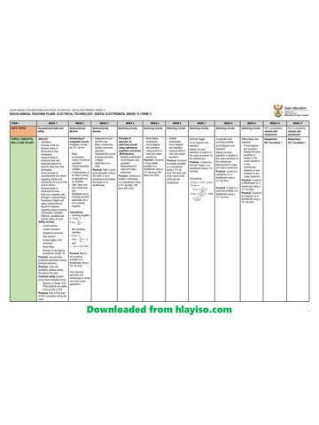
Electrical Technology Grade 12 NSC June 2024 QP (Eng)
Grade 12 Electrical Technology question paper from the NSC June Exam 2024 (English), 33 pages. Read online or download the free PDF.
Electrical Technology · Grade 12 · NSC June Exam · 2024 · English. Question paper, 33 pages. Read online or download the PDF.
- Subject
- Electrical Technology
- Grade
- Grade 12
- Language
- English
- Document type
- Question paper
- Year
- 2024
- Exam period
- NSC June Exam
- Curriculum
- CAPS
- Pages
- 33
- File size
- 1.1 MB
Free to read online, no sign-up needed
Loading document…
Loading document…
1 of 33
This exam
Document textSearch extracted text and jump to a page.
Electrical Technology: Electronics 2 DBE/2023
SC/NSC
INSTRUCTIONS AND INFORMATION
1. This question paper consists of SIX questions.
2. Answer ALL the questions.
3. Answer the following questions on the attached ANSWER SHEETS:
QUESTIONS 4.4.3 and 4.5.3
QUESTIONS 5.3.6, 5.4.3 and 5.6.1
QUESTIONS 6.2.2, 6.6.3 and 6.8.3
4. Write your centre number and examination number on every ANSWER
SHEET and hand them in with your ANSWER BOOK, whether you have used
them or not.
5. Sketches and diagrams must be large, neat and FULLY LABELLED.
6. Show ALL calculations and round off answers correctly to TWO decimal
places.
7. Number the answers correctly according to the numbering system used in this
question paper.
8. You may use a non-programmable calculator.
9. Calculations must include:
9.1 Formulae and manipulations where needed
9.2 Correct replacement of values
9.3 Correct answer and relevant units where applicable
10. A formula sheet is attached at the end of this question paper.
11. Write neatly and legibly.
Copyright reserved Please turn over
Electrical Technology: Electronics 3 DBE/2023
SC/NSC
QUESTION 1: MULTIPLE-CHOICE QUESTIONS
Various options are provided as possible answers to the following questions. Choose
the answer and write only the letter (A–D) next to the question numbers (1.1 to 1.15) in
the ANSWER BOOK, e.g. 1.16 D.
1.1 A critical incident causes …
A damage to equipment. External repair services are required.
B a person to sustain a sudden and severe physical injury. External
medical services are required.
C a person to sustain a physical injury. External medical services are not
required.
D a person to get a mental disturbance. A restful recovery is required. (1)
1.2 The … is the term used for the ratio of the applied voltage to the resulting
circuit current where the applied voltage is the resultant of V R, VC and VL in an
RLC circuit.
A reactance
B resistance
C impedance
D phase angle (1)
1.3 The current through a capacitor in an RLC parallel circuit will … when the
frequency increases.
A remain the same
B decrease
C increase
D be zero (1)
1.4 The … of the inductor is the ratio of the inductor's reactance (XL) to its internal
resistance (rint).
A resonant frequency
B Q-factor
C power
D gain (1)
1.5 If the emitter is supplied with sufficient current, the UJT operating point will
continue falling until the … point is reached.
A zero voltage
B saturation
C cut-off
D valley (1)
Copyright reserved Please turn over
Electrical Technology: Electronics 4 DBE/2023
SC/NSC
1.6 ONE of the advantages of a Darlington transistor, when used in common
collector mode, is that it has …
A lower input impedance.
B high voltage distortion.
C higher output impedance.
D lower output impedance. (1)
1.7 ONE of the characteristics of an ideal op amp is that the input impedance is …
A extremely high.
B zero.
C extremely low.
D moderate. (1)
1.8 When negative feedback is used in an op-amp circuit, the overall gain is …
A increased.
B unchanged.
C reduced.
D infinite. (1)
1.9 The operation of a Schmitt trigger can best be described by …
A hysteresis.
B negative feedback.
C open-loop gain.
D attenuation. (1)
1.10 The … is the only op-amp application that uses an 'open loop' connection to
bring its full gain of ±100 000 into use.
A summing amplifier
B integrator
C comparator
D differentiator (1)
1.11 The … determines the shape of the output in an op-amp integrator circuit.
A input capacitor
B feedback resistor
C input voltage
D RC time constant (1)
Copyright reserved Please turn over
Electrical Technology: Electronics 5 DBE/2023
SC/NSC
1.12 When a square wave is fed to the input of a passive RC differentiator with a
short time constant, the output will be a …
A sine wave with 90º phase shift.
B spike with a fast rise and slow decay.
C square wave with 180º phase shift.
D a triangular wave. (1)
1.13 Tuning circuits in RF amplifiers are primarily …
A class A amplifiers.
B class B amplifiers.
C class AB amplifiers.
D class C amplifiers. (1)
1.14 In an amplifier, the gain that occurs between the lower and upper frequency
range is called the …
A critical gain.
B input gain.
C midrange gain.
D decibel gain. (1)
1.15 An oscillator differs from an amplifier because the oscillator …
A has no gain.
B requires no input signal.
C requires an input signal.
D always has a half-wave output. (1)
[15]
QUESTION 2: OCCUPATIONAL HEALTH AND SAFETY
2.1 State the purpose of the Occupational Health and Safety Act, 1993 (Act 85 of
1993). (3)
2.2 Explain how an unsafe act can reduce the rate of production at the work
place. (2)
2.3 Explain the term high impact; low probability with reference to risk analysis. (2)
2.4 State TWO recommended procedures to stop bleeding in an emergency. (2)
2.5 State ONE procedure to follow for personal protection when administering the
procedures mentioned in QUESTION 2.4. (1)
[10]
Copyright reserved Please turn over
Electrical Technology: Electronics 6 DBE/2023
SC/NSC
QUESTION 3: RLC CIRCUITS
3.1 Describe what is meant by the term in phase with reference to the relationship
between the applied voltage and current in an RLC circuit connected to an
AC supply. (3)
3.2 Refer to the AC waveforms in FIGURE 3.2 below and draw the phasor
diagram that represents them.
+V VL
IL
t
-V
FIGURE 3.2: CURRENT AND VOLTAGE WAVEFORMS (3)
3.3 Name TWO applications of resonance as applicable to tuned circuits. (2)
3.4 Identify the graphs below.
FIGURE 3.4(a) FIGURE 3.4(b)
3.4.1 FIGURE 3.4(a) (1)
3.4.2 FIGURE 3.4(b) (1)
Copyright reserved Please turn over
Electrical Technology: Electronics 7 DBE/2023
SC/NSC
3.5 Refer to FIGURE 3.5 below and answer the questions that follow.
VL= 60 V
VT
θ
I=4A
VR = 30 V
VC = 20 V
FIGURE 3.5: PHASOR DIAGRAM
Given:
VL = 60 V
VC = 20 V
VR = 30 V
I = 4A
f = 60 Hz
3.5.1 Calculate the value of the supply voltage. (3)
3.5.2 Calculate the phase angle. (3)
3.5.3 State whether the phase angle is leading or lagging. (1)
Copyright reserved Please turn over
Electrical Technology: Electronics 8 DBE/2023
SC/NSC
3.6 Refer to FIGURE 3.6 below and answer the questions that follow.
L XC= 113,12 Ω
R = 100 Ω
IT = 1,5 A
150 V/3 kHz
FIGURE 3.6: RLC SERIES CIRCUIT
Given:
R = 100 Ω
XC = 113,12 Ω
VT = 150 V
IT = 1,5 A
f = 3 kHz
3.6.1 Calculate the value of the inductance for the circuit to resonate
at 3 kHz. (3)
3.6.2 Calculate the Q-factor of the circuit at resonance. (3)
3.6.3 Calculate the bandwidth of the circuit. (3)
3.6.4 Explain how the value of the total current would be influenced if R
is halved when the circuit is at resonance. (1)
Copyright reserved Please turn over
Electrical Technology: Electronics 9 DBE/2023
SC/NSC
3.7 Refer to FIGURE 3.7 below and answer the questions that follow.
1,22 A IT 1,2 A IR IL 0,2 A IC
120 V R XL Xc
100 Hz 100 Ω 3 600 Ω
FIGURE 3.7: RLC PARALLEL CIRCUIT DIAGRAM
Given:
VT = 120 V
IR = 1,2 A
IC = 0,2 A
IT = 1,22 A
f = 100 Hz
R = 1 Ω
XC = 6 Ω
XL = 3 Ω
3.7.1 Calculate the current through the inductor. (3)
3.7.2 Calculate the value of the active power. (3)
3.7.3 State, with a reason, if the circuit is capacitive or inductive. (2)
[35]
Copyright reserved Please turn over
Electrical Technology: Electronics 10 DBE/2023
SC/NSC
QUESTION 4: SEMICONDUCTOR DEVICES
4.1 Identify the semiconductor device symbols in QUESTIONS 4.1.1 and 4.1.2
below.
4.1.1 D
G
S (2)
4.1.2 D
G
S (2)
4.2 Describe the construction of the MOSFET in FIGURE 4.2 below.
G
S D
P-substrate
G
FIGURE 4.2: CROSS-SECTION OF A MOSFET CONSTRUCTION (4)
Copyright reserved Please turn over
Electrical Technology: Electronics 11 DBE/2023
SC/NSC
4.3 Refer to FIGURE 4.3 below and answer the questions that follow.
VDD
R1 RD
C2
VOUT
D
C1
VIN G
VIN
S
0 90⁰ 180⁰ R2 RS
0V
FIGURE 4.3: MOSFET AMPLIFIER
4.3.1 State the purpose of R1 and R2. (1)
4.3.2 Describe how the MOSFET can be operated as a linear amplifier. (3)
4.3.3 Describe the operation of the circuit during the first 90º of the input
signal. (3)
Copyright reserved Please turn over
Electrical Technology: Electronics 12 DBE/2023
SC/NSC
4.4 Refer to FIGURE 4.4 below and answer the questions that follow.
ID
VGS
A
ID
+ VGS
Input signal
FIGURE 4.4: TRANSFER CHARACTERISTIC CURVE
4.4.1 Identify the type of transistor used to produce the characteristic
curve in FIGURE 4.4. (1)
4.4.2 Name point A on the characteristic curve. (1)
4.4.3 Draw the output waveform on the ANSWER SHEET for
QUESTION 4.4.3. (2)
Copyright reserved Please turn over
Electrical Technology: Electronics 13 DBE/2023
SC/NSC
4.5 FIGURE 4.5 below shows a UJT as a saw-tooth generator. Answer the
questions that follow.
+ VBB
R1 R2
B2
E
VC B1
C
R3
t
0V
FIGURE 4.5: THE UJT AS A SAW-TOOTH GENERATOR
4.5.1 State the mode of switching of the UJT in FIGURE 4.5. (1)
4.5.2 Explain the purpose of R3. (2)
4.5.3 Draw the output waveform that would develop across B 1 on the
ANSWER SHEET for QUESTION 4.5.3. (3)
4.6 FIGURE 4.6 below shows two identical signals on the input terminals of an op
amp. Draw the output waveform of the op amp in the ANSWER BOOK.
V1 t +V
V1 -
VOUT
V2 +
-V
V2 t
FIGURE 4.6: 741 OP AMP (2)
Copyright reserved Please turn over
Electrical Technology: Electronics 14 DBE/2023
SC/NSC
4.7 Refer to FIGURE 4.7 below and answer the questions that follow.
+9 V
RF
-9V 47 kΩ
VIN VOUT
RIN
10 kΩ
0V
FIGURE 4.7: OPERATIONAL AMPLIFIER CIRCUIT
4.7.1 Identify the op-amp circuit in FIGURE 4.7. (1)
4.7.2 Describe what is meant by infinite bandwidth of an op amp. (2)
4.7.3 Calculate the voltage gain. (3)
4.7.4 Calculate the output voltage if a 100 mV signal is applied to the
input. (3)
Copyright reserved Please turn over
Electrical Technology: Electronics 15 DBE/2023
SC/NSC
4.8 Refer to FIGURE 4.8 below and answer the questions that follow.
Discharge Threshold
+Vcc
Supply A
8 7 6 5
5 kΩ
_
+
Comparator 1
Q
S
Flip-
5 kΩ flop
Comparator 2
R
Q
_
+
Output
5 kΩ driver
Ground 1
2
Output 3
4
Reset
B
FIGURE 4.8: 555 IC TIMER
4.8.1 Label pins A and B. (2)
4.8.2 Explain the function of the discharge input on pin 7. (2)
4.8.3 Explain the function of comparator 1. (3)
4.8.4 State TWO uses of the 555 IC. (2)
[45]
Copyright reserved Please turn over
Electrical Technology: Electronics 16 DBE/2023
SC/NSC
QUESTION 5: SWITCHING CIRCUITS
5.1 FIGURE 5.1 below shows block diagrams with different input and output
states for three types of multivibrators. Identify the multivibrator in each of the
following blocks.
Input X Output
T1 T2
T1 T2
Y Output
Input
T1
T1
No input Z Output
FIGURE 5.1: BLOCK DIAGRAMS OF MULTIVIBRATORS
5.1.1 Block X (1)
5.1.2 Block Y (1)
5.1.3 Block Z (1)
Copyright reserved Please turn over
Electrical Technology: Electronics 17 DBE/2023
SC/NSC
5.2 FIGURE 5.2 below shows the circuit of a multivibrator. Answer the questions
that follow.
R1
1 kΩ
RS
4 8 3
7
9V 5 555 R2
100 kΩ
LED
2 1 6
C2 C1
0,1 µF 10 µF
FIGURE 5.2: MULTIVIBRATOR CIRCUIT
5.2.1 State the purpose of variable resistor R2. (2)
5.2.2 Explain how the LED will be affected if it is directly connected to
pin 3 without resistor RS . (3)
5.2.3 Explain how this circuit operates. (4)
5.2.4 State the discharge path of capacitor C1. (1)
5.3 FIGURE 5.3 below shows a monostable multivibrator circuit using a 741 op
amp. The capacitor is fully charged through resistor R3. Answer the questions
that follow.
R1 R3
4k7 1 kΩ
2 7
6 VOUT
6V
3
4
R2
S 4k7 C
10 µF
0V
FIGURE 5.3: MONOSTABLE MULTIVIBRATOR CIRCUIT
5.3.1 Determine the voltage at pin 2 (inverting input) of the op amp. (2)
Copyright reserved Please turn over
Electrical Technology: Electronics 18 DBE/2023
SC/NSC
5.3.2 Determine the voltage at pin 3 (non-inverting input) when the
switch is open. (1)
5.3.3 State whether the output is high (6 V) or low (0 V) when the switch
is open. Motivate your answer. (2)
5.3.4 Determine the voltage at pin 3 (non-inverting input) when the
switch is pressed. Motivate your answer. (2)
5.3.5 Describe the operation of the circuit with reference to the voltages
on the two input terminals and the output of the op amp when the
switch is pressed. (5)
5.3.6 Refer to FIGURE 5.3.6 below and draw the output waveform on the
ANSWER SHEET for QUESTION 5.3.6.
V
6 VC
4
Input
Inset VR2
2
0
t
FIGURE 5.3.6 (3)
5.4 FIGURE 5.4 below shows a non-inverting Schmitt trigger. Answer the
questions that follow.
+9 V
VOUT
+V
VIN
t -9 V R2
VIN R1
-V
FIGURE 5.4: NON-INVERTING SCHMITT TRIGGER
5.4.1 Determine the voltage at which the circuit will trigger. Motivate your
answer. (2)
5.4.2 Name TWO uses of a Schmitt trigger. (2)
5.4.3 Draw the output signal on the ANSWER SHEET for
QUESTION 5.4.3. (4)
Copyright reserved Please turn over
Electrical Technology: Electronics 19 DBE/2023
SC/NSC
5.5 The information in TABLE 5.5 below was gathered from an inverting summing
amplifier with three inputs. The input resistors are all equal and the feedback
resistance was adjusted by using a variable resistor. Use the data in the table
to answer the questions that follow.
INPUT 1 INPUT 2 INPUT 3 RIN RF VOUT GAIN
(V) (V) (V) (kΩ) (kΩ) (V)
3 1 2 10 X -6 -1
0,3 0,4 0,3 10 100 -10 Y
1 0,5 0,5 10 20 Z -2
TABLE 5.5
5.5.1 Determine the value of the feedback resistance (RF) at X. (1)
5.5.2 Calculate the gain at Y. (3)
5.5.3 Calculate the output voltage (VOUT) at Z. (3)
5.5.4 Deduce from TABLE 5.5 the relationship between RF and the gain. (1)
5.6 Refer to FIGURE 5.6 below and answer the questions that follow.
RF
+V
1 nF +V
VIN
t
VOUT
-V
R1 -V
0V
FIGURE 5.6: OP-AMP DIFFERENTIATOR
5.6.1 Draw the output on the ANSWER SHEET for QUESTION 5.6.1. (4)
5.6.2 Explain what determines the polarity of the output voltage. (2)
[50]
Copyright reserved Please turn over
Electrical Technology: Electronics 20 DBE/2023
SC/NSC
QUESTION 6: AMPLIFIERS
6.1 Define the term stability with reference to the Q-point of amplifiers. (2)
6.25. Refer to FIGURE 6.2 below and answer the questions that follow.
IC
Input signal
Output signal
Q-point
(V)
4 8 12 16 20 VCE
FIGUREF FIGURE 6.2: CLASSES OF AMPLIFICATION
6.2.1 Identify the class of amplification represented in FIGURE 6.2. (1)
6.2.2 Draw the output waveform on the ANSWER SHEET for
QUESTION 6.2.2. (2)
Copyright reserved Please turn over
Electrical Technology: Electronics 21 DBE/2023
SC/NSC
6.3 Refer to FIGURE 6.3 below and answer the questions that follow.
+20 Vcc
Ic
(mA)
6
IB = 140 µA RB RC
5
C IB = 120 µA Vout
4 IB = 100 µA
3 IB = 80 µA
A Q1
IB = 60 µA
2 IB = 40 µA
B RE
IB = 20 µA
1
IB = 0
f (V)
VCE 0V
4 8 12 16 20
TRANSISTOR BIASING
CHARACTERISTIC CURVE
FIGURE 6.3: CHARACTERISTIC CURVE AND TRANSISTOR BIASING
66.3.1 Identify region C in the characteristic curve. (1)
66.3.2 Interpret the data given in FIGURE 6.3 above and calculate the
value of the load resistor. (3)
66.3.3 Explain why the gradient of the load line decreased from A to B
while the supply voltage remained the same. (2)
Copyright reserved Please turn over
Electrical Technology: Electronics 22 DBE/2023
SC/NSC
6.4 Refer to FIGURE 6.4 below and answer the questions that follow.
+9 V
R1 RC
C2
C
C1
B
BC 109
E Earphone
Microphone
R2 RE CE
20 Hz–2 kHz
0V
FIGURE 6.4: RC-COUPLED AMPLIFIER
6.4.1 Determine the value of the voltage drop across RC. (1)
6.4.2 Explain why the circuit in FIGURE 6.4 must be an audio amplifier. (3)
6.4.3 Explain the function of the capacitor CE in parallel with resistor RE. (2)
Copyright reserved Please turn over
Electrical Technology: Electronics 23 DBE/2023
SC/NSC
6.5 Refer to FIGURE 6.5 below and answer the questions that follow.
+ VCC
T1 T2
R1 R3
Q1 Q2
C2 C3
R2 R E1 C1 R4 R E2
0V
FIGURE 6.5: TWO-STAGE TRANSFORMER-COUPLED AMPLIFIER
6.5.1 State TWO functions of capacitors C1 and C3. (2)
6.5.2 State ONE advantage of the transformer-coupled amplifier. (1)
6.5.3 Describe the uses of T1. (3)
Copyright reserved Please turn over
Electrical Technology: Electronics 24 DBE/2023
SC/NSC
6.6 Refer to FIGURE 6.6 below and answer the questions that follow.
+Vcc
Q1
C2
V Q2
Input signal
Speaker
FIGURE 6.6: PUSH-PULL AMPLIFIER CIRCUIT DIAGRAM
6.6.1 State the disadvantage of the amplifier in FIGURE 6.6. (1)
6.6.2 Describe the function of C2. (2)
6.6.3 Draw the output waveform across transistor Q2 on the ANSWER
SHEET for QUESTION 6.6.3. (2)
Copyright reserved Please turn over
Electrical Technology: Electronics 25 DBE/2023
SC/NSC
6.7 Refer to FIGURE 6.7 below and answer the questions that follow.
+VCC
T2
R1 C1 C2 Output
T1
Q1
Input
R2 C3 RE CE
0V
FIGURE 6.7: RADIO-FREQUENCY AMPLIFIER
6.7.1 State the use of the radio frequency amplifier. (2)
6.7.2 With reference to radio frequency amplifiers, state the term used
for unwanted frequencies. (1)
6.7.3 Give the reason for using two LC-tuned circuits instead of one
LC-tuned circuit. (1)
6.7.4 Explain why pre-set capacitors are used in the LC-tuned circuits
instead of ordinary capacitors. (1)
Copyright reserved Please turn over
Electrical Technology: Electronics 26 DBE/2023
SC/NSC
6.8 Refer to FIGURE 6.8 below and answer the questions that follow.
+VCC
RF choke
R1
C2 C4
C3
Q1
VC1
L1 output
C1 R2 R3
C5
t
0V
L2
FIGURE 6.8: HARTLEY OSCILLATOR
6.8.1 State ONE application of the Hartley oscillator. (1)
6.8.2 State the purpose of transistor Q1. (2)
6.8.3 Draw the output waveform of the circuit on the ANSWER SHEET
for QUESTION 6.8.3 when an AC signal is developed across the
capacitor (C1) of the tank circuit. (2)
Copyright reserved Please turn over
Electrical Technology: Electronics 27 DBE/2023
SC/NSC
6.9 Refer to FIGURE 6.9 below and answer the questions that follow.
+VCC
RB RC
C5
VOUT
C1 C2 C3
Q1
R1 R2 R3 R4 C4
0V
FIGURE 6.9: RC PHASE-SHIFT OSCILLATOR
6.9.1 State the function of RC. (2)
6.9.2 Calculate the value of the capacitor when the oscillation frequency
of the RC phase-shift oscillator is 64,98 Hz with a resistor value of
1 kΩ. (3)
6.9.3 Will the oscillation frequency of the circuit decrease or increase
when the values of the capacitors in the phase-shift network
decrease? Motivate your answer. (2)
[45]
TOTAL: 200
Copyright reserved
Electrical Technology: Electronics DBE/2023
SC/NSC
FORMULA SHEET
RLC CIRCUITS SEMICONDUCTOR DEVICES
= os θ VOUT R RF
XL 2 fL Gain A V F AV 1
VIN RIN RIN
1
XC T= ( )
2 fC
fr
1 OR fr f2 f1
2 LC 2 T= (1 )
fr
BW OR BW f2 f1
Q SWITCHING CIRCUITS
Series R R R
VOUT V1 F V2 F ...VN F
VR I R R1 R2 RN
VL I XL VOUT VOUT
Gain A V
VC I XC VIN V1 V2 ...VN
VT IT IR IC IL VOUT (V1 V2 ...VN )
IT OR
Z AMPLIFIERS
V
Z R 2 X L X C
2
IC C VCC VCE ICRC
RC
VT VR VL VC VT I Z VB VBE VRE
2 2
OR
R VR V - VC VOUT
Cos θ OR Cos θ OR Tan θ L AV
Z VT VR VIN
XL XC VL VC 1 L I
Q A I OUT
R R VT VT R C IIN
Parallel P
A P OUT AP A V A I
VT VR VL VC PIN OR
VT
IR βT = β1 x β2 OR A VT A V1 A V2 A V3 ...A Vn
R
VT
IC PIN I2 ZIN POUT I2 Z OUT
XC AND
V Oscillation frequency
IL T
XL OR
√ √
IT IR IL IC
2 2
GAIN IN DECIBELS
VT I
Z A I 20log10 OUT
IT IIN
I VOUT
Cos θ R A V 20log10 OR A V 20log 10 A VT
IT VIN
R R POUT P2
Q A P 10log10 OR A P 10log10
XL X C PIN P1
Copyright reserved
Electrical Technology: Electronics DBE/2023
SC/NSC
CENTRE NUMBER:
EXAMINATION NUMBER:
ANSWER SHEET
QUESTION 4: SEMICONDUCTOR DEVICES
4.4.3
ID
VGS
Output signal
A
ID
VGS
Transfer mark to
answer book
Input signal
FIGURE 4.4.3 MOD (2)
4.5.3
VC
t
VR2
Transfer mark to
answer book
t
FIGURE 4.5.3 MOD (3)
Copyright reserved
Electrical Technology: Electronics DBE/2023
SC/NSC
CENTRE NUMBER:
EXAMINATION NUMBER:
ANSWER SHEET
QUESTION 5: SWITCHING CIRCUITS
5.3.6 V
6 VC
4
Input VR2
2
0
t
V
6
4
Output
Transfer mark to
2 answer book
0
t
FIGURE 5.3.6 MOD (3)
5.4.3 +V
VIN
t
-V
+VSAT
VOUT
t Transfer mark to
answer book
-VSAT
FIGURE 5.4.3 MOD (4)
Copyright reserved
Electrical Technology: Electronics DBE/2023
SC/NSC
CENTRE NUMBER:
EXAMINATION NUMBER:
ANSWER SHEET
5.6.1
+V
VIN
t
-V
+V
VOUT Transfer mark to
t answer book
-V
FIGURE 5.6.1 MOD (4)
Copyright reserved
Electrical Technology: Electronics DBE/2023
SC/NSC
CENTRE NUMBER:
EXAMINATION NUMBER:
ANSWER SHEET
QUESTION 6: AMPLIFIERS
6.2.2
IC
Input signal
Output signal
Q-point
(V)
4 8 12 16 20 VCE
Transfer mark to
answer book
FIGURE 6.2.2 MOD (2)
6.6.3
+V
t
Transfer mark to
answer book
-V
FIGURE 6.6.3 MOD (2)
Copyright reserved
Electrical Technology: Electronics DBE/2023
SC/NSC
CENTRE NUMBER:
EXAMINATION NUMBER:
ANSWER SHEET
6.8.3
VC1
t
Output
waveform t
Transfer mark to
answer book
FIGURE 6.8.3 MOD (2)
Copyright reserved
Study this subject
Recommended for this subject
Question paper
Electrical Technology Grade 12 NSC June 2024 QP (Eng)
Memorandum
Electrical Technology Grade 12 Eastern Cape Prelim 2024 Memo
Memorandum
Electrical Technology Grade 12 Eastern Cape Prelim 2024 Memo
Memorandum
Electrical Technology Grade 12 Eastern Cape Prelim 2024 Memo
Question paper
Electrical Technology Grade 12 Eastern Cape Mock 2023 QP
Question paper
Electrical Technology Grade 12 Eastern Cape Mock 2022 QP
More from Grade 12 Electrical Technology
Annual teaching plan
Gr 12 Dig Elec ATP 2023 24
Memorandum
Electrical Technology Grade 12 Eastern Cape Mock 2025 Memo
Memorandum
Electrical Technology Grade 12 P1 Gauteng June 2025 Memo
Memorandum
Electrical Technology Grade 12 NSC November 2025 Memo (Afr)
Memorandum
Electrical Technology Grade 12 Eastern Cape Mock 2023 Memo
Memorandum