
NATIONAL
SENIOR CERTIFICATE
GRADE 12
ELECTRICAL TECHNOLOGY: ELECTRONICS
NOVEMBER 2024
MARKING GUIDELINES
MARKS: 200
These marking guidelines consist of 16 pages.
Copyright reserved Please turn over
Skip to contentAll 2024 papers 
View all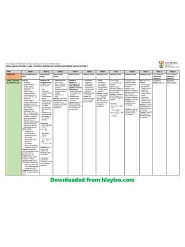
Electrical Technology Grade 12 November 2024 NSC Memo (Eng)
Grade 12 Electrical Technology memorandum from the November 2024 NSC (English), 16 pages. Read online or download the free PDF.
Electrical Technology · Grade 12 · November 2024 NSC · 2024. Memorandum. Read online or download the PDF.
- Subject
- Electrical Technology
- Grade
- Grade 12
- Document type
- Memorandum
- Year
- 2024
- Exam period
- November 2024 NSC
- Curriculum
- CAPS
- Pages
- 16
- File size
- 434.9 KB
Free to read online, no sign-up needed
Loading document…
Loading document…
1 of 16
This exam
Document textSearch extracted text and jump to a page.
Electrical Technology: Electronics 2 DBE/November 2024
NSC – Marking Guidelines
INSTRUCTIONS TO THE MARKERS
1. All questions with multiple answers imply that any relevant, acceptable
answer should be considered.
2. Calculations:
2.1 All calculations must show the formulae.
2.2 Substitution of values must be done correctly.
2.3 All answers MUST contain the correct unit to be considered.
2.4 Alternative methods must be considered, provided that the correct
answer is obtained.
2.5 Where an incorrect answer could be carried over to the next step,
the first answer will be deemed incorrect. However, should the
incorrect answer be carried over correctly, the marker has to re-
calculate the values, using the incorrect answer from the first
calculation. If correctly used, the candidate should receive the full
marks for subsequent calculations.
3. These marking guidelines is only a guide with model answers. Alternative
interpretations must be considered and marked on merit. However, this
principle should be applied consistently throughout the marking session at
ALL marking centres.
Copyright reserved
Electrical Technology: Electronics 3 DBE/November 2024
NSC – Marking Guidelines
QUESTION 1: MULTIPLE CHOICE
1.1 B✓ (1)
1.2 A✓ (1)
1.3 B✓ (1)
1.4 A✓ (1)
1.5 C✓ (1)
1.6 B ✓ (1)
1.7 D✓ (1)
1.8 B✓ (1)
1.9 B✓ (1)
1.10 C✓ (1)
1.11 C✓ (1)
1.12 B/C ✓ (1)
1.13 B✓ (1)
1.14 D✓ (1)
1.15 C✓ (1)
[15]
Copyright reserved Please turn over
Electrical Technology: Electronics 4 DBE/November 2024
NSC – Marking Guidelines
QUESTION 2: OCCUPATIONAL HEALTH AND SAFETY
2.1 Workplace means any premises or place where a person performs work ✓ in
the course of employment. ✓ (2)
2.2 Your right to fair labour practices. ✓
Your right to work reasonable hours. ✓
Your right to belong to a trade union.
Your right to earn a living wage.
Your right not to be discriminated against.
Your right to work in a safe environment. (2)
2.3 Poor ventilation reduces the correct amount of oxygen ✓ which might lead
to drowsiness. ✓
NOTE: If reference is made to other effects that relates to poor ventilation like
drowsiness, accidents etc. the answer will be accepted on merit. (2)
2.4 • To dismiss an employee without due process.
• To reduce the rate of remuneration without due process.
• Alter the terms of conditions of his/her employment to terms of conditions
that is less favourable to him/herself.
• Harassment and verbal abuse.
• Alter position relative to other people.
• Treat employees unfair because of race.
NOTE: If a learner only mentions an infringement of rights only 1 mark will be
awarded. Duplicate mentioning of rights will not be awarded. (2)
2.5 Equipment may be damaged making it unsafe endangering the life of other
users which might lead to an accident/injury. (2)
[10]
Copyright reserved Please turn over
Electrical Technology: Electronics 5 DBE/November 2024
NSC – Marking Guidelines
QUESTION 3: RLC CIRCUITS
3.1 3.1.1 Inductive reactance is the opposition to the flow of current ✓ when
an inductor is connected to an ac supply. ✓
Inductive reactance is the opposition offered to the flow of
alternating current by an inductor. (2)
3.1.2 Bandwidth is the range of frequencies ✓ for which the circuit output
voltage (or) current value equals 70,7 % or more of its maximum
amplitude. ✓
NOTE: A band of frequencies centred around the resonant
frequency without mentioning 70,7% of the amplitude will be
awarded 1 mark.
The bandwidth of an RLC circuit refers to the range of frequencies
over which an RLC circuit effectively responds to an input signal
and transmits more than 50% of the power to a load. (2)
3.2 3.2.1 Lagging ✓ (1)
3.2.2 𝑉𝐿 = 𝐼𝑋𝐿 ✓
𝑉𝐿
𝐼=
𝑋𝐿
3,45 ✓
=
150
= 23 𝑚𝐴 ✓
= 0,023 𝐴 (3)
3.2.3 𝑋𝐿 = 2𝜋𝑓𝐿 ✓
𝑋𝐿
𝐿=
2𝜋𝑓
150 ✓
=
2𝜋(50)
= 477,46 𝑚𝐻
✓
= 0,48 𝐻
(3)
3.2.4 𝑍 = √𝑅 2 + (𝑋𝐿 − 𝑋𝐶 )2 ✓
𝑅 = √𝑍 2 − (𝑋𝐿 − 𝑋𝐶 )2
✓
= √106,422 − (150 − 113,6)2
= 100 Ω ✓ (3)
3.2.5 VL ✓
✓
VT
(VL – VC)
θ ✓
IT VR
Rotation
✓
VC
NOTE: Rotation and VT are compulsory marks, thereafter any two
correctly placed labels.
XL and XC will not be accepted as the given diagram to
complete from the question paper indicated voltage values. (4)
Copyright reserved Please turn over
Electrical Technology: Electronics 6 DBE/November 2024
NSC – Marking Guidelines
3.2.6 A decrease in frequency caused the inductive reactance to
decrease ✓ and the capacitive reactance to increase. ✓ When
these two values move closer to one another their effects cancel
each other out decreasing the impedance ✓ causing the current to
increase and the phase angle to decrease. (3)
3.3 3.3.1 𝑉𝑇 ✓
𝐼𝑅 =
𝑅
230 ✓
=
60
= 3,83 𝐴 ✓ (3)
3.3.2 𝑉𝑇 ✓
𝑋𝐶 =
𝐼𝐶
✓
230
=
9,2
= 25 Ω ✓ (3)
3.3.3 IT = IR = 3,83 A ✓
XC = XL which indicates that the ✓
circuit is at resonance (2)
3.3.4 XC = XL
𝑅 ✓
𝑄=
𝑋𝐿
✓
60
=
25
= 2,4 ✓ (3)
3.3.5 𝑓𝑟 ✓
𝐵𝑊 =
𝑄
✓
50
=
2,4
= 20,83 𝐻𝑧 ✓ (3)
[35]
Copyright reserved Please turn over
Electrical Technology: Electronics 7 DBE/November 2024
NSC – Marking Guidelines
QUESTION 4: SEMICONDUCTOR DEVICES
4.1 P-channel ✓ enhancement ✓ MOSFET (2)
4.2 4.2.1 The pinching state is reached by increasing the gate to source
voltage, ✓ which widens the depletion regions on both sides of the
channel, ✓ resulting in the drain current (ID) being reduced. ✓ (3)
4.2.2 The Junction field effect transistor (JFET) operates with its gate-
source junction ✓ reverse–biased ✓ which makes the input
resistance at the gate very high whilst the bipolar junction transistor
operates with the forward biased base-emitter junction ✓ which
result in a lower resistance. (3)
4.3 4.3.1 MOSFET transfer ✓ characteristic curve
MOSFET transconductance characteristic curve (1)
4.3.2 A – Cut-off region ✓
B – Enhancement region ✓ (2)
4.3.3 • When the input gate-source voltage (VGS) is low✓, the channel
drain current (ID) is low. ✓
• When the gate-source voltage rises, ✓ the channel widens and
the drain current increases. ✓
NOTE: If a candidate mentions that VGS and ID are directly
proportional 2 marks will be awarded and any of the two bullets
above can be mentioned for the other 2 marks. (4)
4.3.4 Amplifier ✓
Switch ✓ (2)
4.4 The JFET only operates in the depletion mode. ✓
The MOSFET operates in both depletion and enhancement modes. (1)
4.5 4.5.1 Positive pulse. ✓ (1)
4.5.2 When the emitter is supplied with sufficient current, ✓ the operating
point will continue falling ✓ from the peak point until it reaches the
valley point.
When VE VX , the operating point will fall from the peak point until
it reaches the valley point. (2)
4.5.3 (a) Unijunction transistor (UJT) consists of a single PN -junction✓
whilst a bipolar junction transistor (BJT) consists of two
PN-junctions ✓ called Emitter Base Junction and Collector-
Base junction. (2)
(b) The unijunction transistor is essentially a voltage controlled
switch and does not have amplifying properties. ✓ The
Bipolar Junction transistor (BJT) is current operating device
and has amplifying properties. ✓ (2)
Copyright reserved Please turn over
Electrical Technology: Electronics 8 DBE/November 2024
NSC – Marking Guidelines
4.6 4.6.1 FIGURE A - output voltage will be positive/high. ✓
FIGURE B - output voltage will be negative/low. ✓ (2)
4.6.2 Small size ✓
Cheap ✓
Low power consumption
Highly stable
Highly reliable (2)
4.6.3 Common mode rejection ratio is the ability of an op-amp to
suppress common mode signals. ✓
The common mode rejection ratio is the ratio between the output
voltage to the common input voltage when the same signal is
applied simultaneously to both inputs. (1)
4.7 4.7.1 Negative feedback. ✓ (1)
4.7.2 𝑅𝐹 ✓
𝐴𝑉 = −
𝑅𝐼𝑁
4 700 ✓
=−
470
= −10 ✓
(3)
4.7.3 𝑉𝑂𝑈𝑇 = 𝐴𝑉 × 𝑉𝐼𝑁 ✓ 𝑅𝑓
𝑉𝑂𝑈𝑇 = 𝑉𝐼𝑁 × (− )
= −10 × 2 × 10−3 𝑅𝐼𝑁
✓ OR
= −0,02𝑉 4700
𝑉𝑂𝑈𝑇 = 0,002 × (− )
✓ 470
= −20 𝑚𝑉
𝑉𝑂𝑈𝑇 = −0,02 𝑉
(3)
4.7.4 The output voltage will be able to swing above ✓ and below ✓ the
zero levels. (2)
4.8.1 Controlling the positioning of a servo device. ✓
Temperature measurement.
Timers in oven temperature control.
Oscillator as motor speed control. (1)
4.8.2 ̅ from the
The NPN transistor (T1) will only turn on when output Q
flip-flop goes high. ✓ (1)
4.8.3 When the inverting terminal voltage is higher - the comparator's
output will be low. ✓ (1)
4.8.4 It divides the supply voltage into three equal values. ✓
The resistors act as voltage dividers. (1)
Copyright reserved Please turn over
Electrical Technology: Electronics 9 DBE/November 2024
NSC – Marking Guidelines
4.8.5 The 555 IC will be triggered ✓ and the output voltage at Pin 3 rises
near to the supply voltage ✓
NOTE: Due to the error in the schematic diagram of the 555 IC, the
following response will be accepted:
When pin 2 falls below ⅓VCC, the output of comparator C2 will be
low, if R of the flip-flop is high, the circuit will be reset, if R is low,
the circuit will stay in its previous state. (2)
[45]
QUESTION 5: SWITCHING CIRCUITS
5.1 Negative feedback is when a portion of the output signal ✓ is fed back to the
input, out of phase ✓ or subtracted from the input. (2)
5.2 5.2.1 Schmitt trigger ✓ (1)
5.2.2 Bistable multivibrator ✓ (1)
5.2.3 Monostable multivibrator ✓ (1)
5.3 5.3.1 R2 is a pull-up resistor ✓
R2 keeps the voltage on pin 2 high. (1)
5.3.2 • When S2 is pressed it connects pin 2 to 0 V. ✓
• This low input triggers the circuit and the output goes high. ✓
• When output goes high LED2 is forward biased and switched
ON. ✓
• while LED1 is reversed biased and switched OFF. ✓ (4)
5.3.3 The circuit is reset by pressing S1. ✓ This connects reset pin 4
to 0 V. ✓ (2)
5.4 5.4.1 0V✓ (1)
5.4.2 During its natural resting condition, the negative reference voltage
keeps the potential on the inverting input negative ✓ ensuring that
the output remains stable at +VCC. ✓ (2)
5.4.3 When a positive trigger voltage greater than VREF is applied to the
inverting input its potential will be greater than the 0 V on the non-
inverting input ✓ causing the output to saturate to – VCC ✓ where it
will remain for the duration of the time constant determined by
C2 and R2. ✓ (3)
Copyright reserved Please turn over
Electrical Technology: Electronics 10 DBE/November 2024
NSC – Marking Guidelines
5.4.4 Trigger pulse
0 1 2 3 4 5 6 t (s)
✓ ✓
+9V
VOUT
t (s)
✓ ✓
-9V
NOTE: 1 mark for starting the output at +9 V
1 mark for the output changing from +9 V to -9 V at trigger
input
1 mark for the correct duration of the output state
1 mark for the return to +9 V (4)
An inverted waveform will loose 1 mark for orientation.
5.5 5.5.1 RF ✓
+supply
2 7
741
6 Output
3
4
R1 ✓
- supply
✓ ✓
C1 R2
(4)
5.5.2 The output voltage of a 741 op-amp astable multivibrator circuit
constantly changes between + VCC and -VCC ✓ where the output of
a 555 IC astable multivibrator circuit changes between +VCC
and 0 V. ✓ (2)
5.6 5.6.1 Variable resistor/Potentiometer R2 ✓ (1)
5.6.2 Resistor R1 ✓
Thermistor ✓ (2)
5.6.3 By adjusting variable resistor R2 ✓ the new reference voltage at
the inverting input will change. ✓ (2)
5.7 Clean up signals in radio receivers. ✓
Eliminate noise caused by switch bounce in digital circuits. ✓
Changing of sine waves into square or rectangular waves
Signal recovery after severe distortion. (2)
Copyright reserved Please turn over
Electrical Technology: Electronics 11 DBE/November 2024
NSC – Marking Guidelines
5.8 5.8.1 Variable resistor R4 provides negative feedback ✓ that controls the
gain of the circuit. ✓ (2)
5.8.2 𝑅𝐹 𝑅𝐹 𝑅𝐹 ✓
𝑉𝑂𝑈𝑇 = − (𝑉1 + 𝑉2 + 𝑉3 )
𝑅1 𝑅2 𝑅3
72000 72000 72000 ✓
= − (0,5 × + 0,45 × + 0,3 × )
10000 10000 10000
= −9 𝑉 ✓
(3)
NOTE: Due to the error on the formula sheet provided, the
following calculation will be accepted.
𝑅𝐹 𝑅𝐹 𝑅𝐹
𝑉𝑂𝑈𝑇 = − (𝑉1 + 𝑉1 + 𝑉1 )
𝑅1 𝑅2 𝑅3
72000 72000 72000
= − (0,5 × + 0,5 × + 0,5 × )
10000 10000 10000
= −10,8 𝑉
5.8.3 When RF = R1 = R2 = R3. ✓ They cancel each other out in the
formula giving VOUT = -(V1+V2+V3).
When R4 is set to 10 kΩ the overall circuit gain is 1. (1)
5.8.4 When R4 is increased beyond 72 kΩ the gain of the amplifier
increases ✓ driving it into saturation and causing distortion on the
output. ✓
NOTE: Because of the formula provided on the formula sheet a
reason in-line with the calculated answer in 5.8.2 will be accepted.
e.g. The circuit is already in saturation, when R4 is increased the
output voltage will remain at a maximum of 9 V. (2)
5.9 5.9.1 A passive differentiator primarily performs mathematical
differentiation on an input signal, ✓ producing an output voltage
proportional to the rate of change of the input voltage. ✓ (2)
Copyright reserved Please turn over
Electrical Technology: Electronics 12 DBE/November 2024
NSC – Marking Guidelines
5.9.2
VIN
0
✓
VOUT
✓
0
✓
NOTE: The wave shape must be correct before any marks are
allocated
1 mark for orientation
1 mark for each ½ cycle (3)
5.10 In an op-amp differentiator a capacitor is connected to the inverting input and
resistor used in the feedback loop. ✓
In an op-amp integrator a resistor is connected to the inverting input with a
capacitor in the feedback loop. ✓ (2)
[50]
Copyright reserved Please turn over
Electrical Technology: Electronics 13 DBE/November 2024
NSC – Marking Guidelines
QUESTION 6: AMPLIFIERS
6.1 Attenuation refers to a circuit with a output voltage smaller ✓ than the input
voltage. ✓
Attenuation is the reduction in signal voltage as it passes through a circuit
and corresponds to a gain of less than 1. (2)
6.2 6.2.1 DC load line is the line on the output characteristic of a transistor
circuit showing the operating points of the amplifier. ✓ (1)
6.2.2 VCE will be equals to VCC = 12 V.✓ (1)
6.2.3 For class A amplification, the quiescent voltage is 6 V.✓
The value of the quiescent voltage is half ✓ the value of the supply
voltage i.e ½ VCC. (2)
6.2.4
IC (mA)
15
10
Q-Point ✓
5
✓
VCE
2 4 6 8 10 12 14 16
FIGURE A (2)
6.3 6.3.1 RC coupled amplifier. ✓ (1)
6.3.2 Roll-off is the rate at which the gain decreases at high
frequencies.✓ (1)
6.3.3 (a) At high frequencies, the reactance of the small parasitic
capacitances of the transistors ✓ becomes lower ✓ and
lower, reducing the gain. (2)
(b) At low frequencies the coupling capacitor's reactance
rises, ✓ blocking more of the signal ✓ and also the
reactance of the decoupling capacitors with the emitter
resistance limit the gain. (2)
Copyright reserved Please turn over
Electrical Technology: Electronics 14 DBE/November 2024
NSC – Marking Guidelines
6.4 6.4.1 Transformer coupled ✓ amplifier. (1)
6.4.2 AC relay ✓
AC motor ✓
Piezo Buzzer (2)
6.4.3 • To match the two impedances and separate the dc circuits.✓
• To couple the output of Q1 to the input of Q2. (1)
6.4.4 There would be no maximum power transfer to the loudspeaker ✓
because the output impedance of the amplifier ✓ does not match
with the input impedance of the speaker ✓ thus meaning the
output sound will be softer. (3)
6.5 6.5.1 Complementary ✓ Push pull amplifier. (1)
6.5.2 Block DC signals ✓ and allows the AC signals to pass
through. ✓
The capacitor couples the circuit with the speaker and acts as a
short term power source for the PNP transistor during each
negative half cycle. (2)
6.5.3
+V
0
t
-V
+V
✓
0
t
✓
-V ✓
(3)
NOTE: 1 mark for each half cycle = 2
1 mark for amplification
Copyright reserved Please turn over
Electrical Technology: Electronics 15 DBE/November 2024
NSC – Marking Guidelines
NOTE: 1 mark for same phase on negative half-cycle
1 mark for NO amplification shown.
6.6 6.6.1 The purpose of transistor Q1 is to amplify the input signal to a value
that drives the tank circuit to oscillation. ✓ (1)
6.6.2 By varying capacitors C1 and C2, the tuned circuit will resonate at
different frequencies, ✓ therefore changing range of frequencies.✓ (2)
6.6.3 ✓
Maximum gain at
resonant frequency
Gain
✓
0,707 X Max Gain
Band pass ✓
fr ✓ Frequency
(4)
6.7 6.7.1 The transistor will be driven alternately on and off,✓ which in turn
continually charges the tank circuit ✓ keeping it oscillating at a
constant ✓ amplitude. (3)
6.7.2 • Block dc current from passing ✓ and allow the AC signal to
pass. ✓
• The coupling capacitors C2 and C3 only allows a Radio
frequency signal from the amplifier to the tank circuit and back. (2)
Copyright reserved Please turn over
Electrical Technology: Electronics 16 DBE/November 2024
NSC – Marking Guidelines
6.8 6.8.1 The values of the capacitors (C1,C2,C3) and resistors (R1,R2,R3) are
selected in such a way that each RC combination ✓ produces a
phase shift of 60o.✓ (2)
6.8.2 RC phase-shift oscillator and Radio-frequency amplifier operates at
a desired frequency ✓ and blocks/suppresses all other
frequencies. ✓
The RC phase-shift oscillator and Radio-frequency amplifier both
rely on resonant/phase shift networks to control their operating
frequencies. (2)
6.9 RC-phase shift oscillators use resistors and capacitors (RC timing circuit) in
the feedback network. ✓
LC oscillator uses capacitors and inductors in their feedback network. ✓ (2)
[45]
TOTAL: 200
Copyright reserved
Study this subject
Recommended for this subject
Question paper
Electrical Technology Grade 12 November 2024 NSC QP (Eng)
Question paper
Electrical Technology Grade 12 November 2024 NSC QP (Afr)
Question paper
Electrical Technology Grade 12 November 2024 NSC QP (Afr)
Memorandum
Electrical Technology Grade 12 Eastern Cape Prelim 2024 Memo
Question paper
Electrical Technology Grade 12 Eastern Cape Prelim 2024 QP
Question paper
Electrical Technology Grade 12 Eastern Cape Prelim 2024 QP
More from Grade 12 Electrical Technology
Annual teaching plan
Gr 12 Dig Elec ATP 2023 24
Question paper
Electrical Technology Grade 12 Gauteng June 2025 QP (Eng)
Question paper
Electrical Technology Grade 12 Eastern Cape Prelim 2024 QP
Question paper
Electrical Technology Grade 12 NSC June 2024 QP (Eng)
Question paper
Electrical Technology Grade 12 NSC June 2024 QP (Eng)
Memorandum